<img alt="" src="https://secure.inventiveinspired7.com/792550.png" style="display:none;">
Skip to the main content.

Ultimate Guide To
PCB Testing

PCB assembly testing methods are an integral part of the manufacturing process.

The testing methods and investigation of each failure are adapted and improved upon regularly. Here we share details on the various classes of electronics and a variety of PCB testing methods. This guide is intended to provide an accurate and informative collection of this information. 

classes of electronics


Complete Guide to PCB Assembly Testing Methods

Making sure your printed circuit boards (PCBs) meet quality standards isn’t just a box to check — it’s the foundation of your product’s success. PCB assembly testing is what ensures that every component functions as intended, catching potential defects early and paving the way for reliable, long-lasting performance in the field.

Whether you’re producing consumer electronics or life-saving medical devices, the right testing approach can protect your timeline, budget, and reputation. In this guide, we’ll walk through the full landscape of PCB testing methods, from basic inspections to advanced failure analysis — so you can make informed decisions that keep your products performing at their best.

classes of electronics

IPC CLASS DEFINITIONS
(FOR CLASS 1, 2, & 3 ELECTRONICS)

Your testing strategy should align with your product's reliability requirements. IPC standards define three distinct classes:

Class 1: General Electronics

This class includes boards with the lowest quality requirements and is mostly found in products with an expected short life cycle.

These electronics are usually found in inexpensive, high-volume productions.

Examples: Toys, basic consumer gadgets


Class 2: Dedicated Service Electronics

Class 2 electronic devices encompass all electronics where continued performance and an extended life cycle are required -- to a point. Uninterrupted service is desired, but not critical.

Along with what's in the chart above, IPC Class 2 examples include:

  • Air conditioners
  • TVs
  • Tablets

In other words, these are items where an early life cycle failure would have you frustrated, but wouldn’t put your life at risk.

Class 3: High-Reliability Electronics

The third class of circuit boards is subject to strict guidelines due to their importance in the field. Class 3 electronics are typically mission-critical products.

Whether it’s a pacemaker or a military radar, a product that needs to meet IPC Class 3 requirements must use high-reliability electronic components to ensure uninterrupted service.

These electronics are usually of the highest quality. Many OEM products that could pass as Class 2 opt for the IPC Class 3 standard because the benefits of higher-quality electronics outweigh the cost of additional testing and inspection.

electronics manufacturing compliance guide
PCB Design Issues

PCB Design Issues

Even with perfect materials, errors can occur during the PCB manufacturing process or stem from flaws in the initial design. These defects can severely compromise the board's functionality and longevity.

Common manufacturing and design defects include:

  • Solder reflow problems
  • Thermo-mechanical failures
  • Component placement errors
  • Trace damage
  • Inadequate trace width.
  • Poor component selection
  • Insufficient thermal management
PCB Environmental Factors

Environmental Factors

Environmental factors, such as extreme heat, dust, and moisture, can lead to failure. Electrostatic discharge during assembly is another common issue that results in premature failure of the circuit board. Human error and an accidental drop can also cause failure.

PCB Life Cycle

Product Lifecycle

Stopping age-related failures is a bit more difficult, and it comes down to preventative maintenance more so than repair. However, if a part does fail, instead of tossing out the entire board, it can be more cost-effective to replace old parts with new ones.

WHAT CAUSES PCB FAILURE?

What to Do When Your PCB Fails


PCBs fail. It’s going to happen.

The best strategy from here? Do everything you can to avoid a repeat by performing a printed circuit board failure analysis. This can pinpoint the exact problem and help prevent it from plaguing other current or future boards.

Understanding what causes PCB failures helps you select the right testing methods.

Common causes include:

Micro-sectioning analysis

Microsection analysis is a destructive test. So it’s performed on a sample of PCBs, not the entire manufacturing run.

The test allows evaluation of the plated through-holes and the lamination. It also examines a part of an assembled PCB for problems such as such as:

  • Thermo-mechanical failures
  • Solder reflow-related failures
  • Shorts
  • Opens
  • Defective components
Micro Sectioning of a PCB


Contaminated PCB


PCB CONTAMINATION TESTING

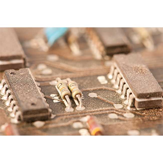
Contamination is one of the most common causes of component failure, even in clean room environments.

Tests to detect contamination include:

  • Resistivity of Solvent Extract (ROSE) testing
  • Fourier Transform Infrared (FTIR) Spectroscopy
  • Ion Chromatography (IC)

X-ray inspection

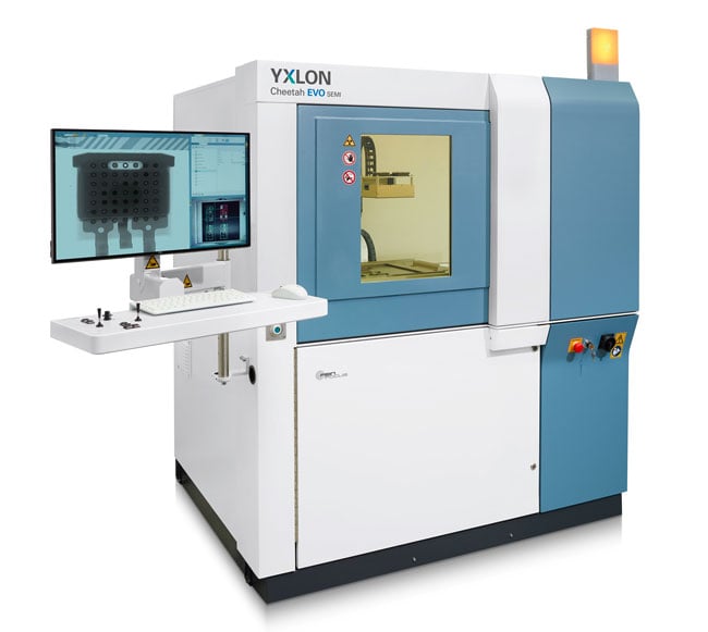
X-ray testing can check elements that are usually hidden from view, such as connections and ball grid array packages with solder joints underneath the chip package.

During this test, an X-ray technician is able to locate defects early during the manufacturing process by viewing:

  • Solder connections
  • Internal traces
  • Barrels
PCB X-Ray Inspection Machine


7 TYPES OF PCB TESTING METHODS

PCB assembly testing is an integral part of the manufacturing process. Reputable electronics contract manufacturers (ECMs) offer a variety of PCB testing methods:

  1. In-circuit testing
  2. Flying probe testing
  3. Automated optical inspection (AOI)
  4. Burn-in testing
  5. X-ray inspection
  6. Functional testing
  7. Other functional testing (solderability, contamination, and more)

number 1

In-Circuit Testing

In-circuit testing (ICT) is one of the strongest types of PCB testing.

An ICT, also known as a bed-of-nails test, powers up and actuates the individual circuitry on the board. It enables functional testing of the various ICs and key components, verifying that signals, voltages, and overall performance meet design specifications.

ICT is often used for complicated designs and/or congested areas that a flying probe would not be able to access effectively.

This test is for a “mature” product with very few revisions expected.  

number 2

Flying Probe Testing

Flying probe testing is a tried-and-true option that’s less expensive than in-circuit testing. It’s a nonpowered type of test that checks for:

  • Opens
  • Shorts
  • Resistance
  • Capacitance
  • Inductance
  • Diode issues

The test uses needles attached to a probe on an x-y grid obtained from basic CAD. Your ECM programs coordinates to match the circuit board and then runs the program.

In some cases, ICT makes it unnecessary to use flying probe testing, but the PCB has to be designed to fit with the test fixture — which means a higher initial cost. While flying probe testing can be cheaper initially, it may actually be less cost-effective for large orders.

One final word of caution: A PCB flying probe test does not power up the board.

number 3

Automated Optical Inspection (AOI)

AOI uses either a single 2D camera or dual 3D cameras to capture images of the PCB. The system then compares these images to known good examples of the circuit. If deviations exceed the expected margin of error, the board is flagged for further inspection by a technician.

AOI can be useful for detecting issues early to ensure production is shut down ASAP. However, it doesn’t power up the board and may not offer 100% coverage for all part types. 


number 4

Burn-In Testing

As the name suggests, burn-in testing is a more intense type of testing for PCBs. It’s designed to detect early failures and establish load capacity. Because of its intensity, burn-in testing can be destructive to the parts.

This is done by running a power supply through the electronics at an elevated

ed temperature, often at its maximum-specified capacity.

Electronics have a higher failure rate close to launch, leveling out in the middle and rising again as they reach the end of the life cycle. If a PCB with an infant mortality failure like this were to make its way into military or medical equipment, it could result in a serious accident.

Burn-in testing reduces the number of latent defects by triggering them through heat, resulting in a more reliable batch of electronics for the OEM. The trade-off is a smaller yield and potentially reduced product lifespan.

The data collected through this process can, in turn, help engineers understand what caused the defects and modify the design to improve product reliability before it even hits burn-in.

number 5

X-Ray Inspection

Also referred to as AXI, this type of “testing” is really more of an inspection tool, at least for most ECMs.

There are 2D and 3D AXI tests, with 3D offering a faster testing period.

X-ray testing checks elements that are usually hidden from view, such as connections and ball grid array packages with solder joints underneath the chip package. While this check can be very useful, it does require trained, experienced operators.

number 6

Functional Testing

Some customers do like a good, old-fashioned functional test. Your ECM uses this to verify that the product will power up.

This test does require a few things:

  • External pieces of equipment
  • Fixtures
  • Requirements for UL, MSHA, and other standards

This functional test and its parameters are usually provided by the customer. Some ECMs can help develop and design such a test.

It does take time. If you want to get your product out the door quickly, this may not be your best choice. But from a quality and longevity standpoint, functional testing can save face and save money. 

number 7

Other Functional Tests

There are other types of functional tests that can be used to check your PCB, depending on the circumstances.

A PCB functional test verifies a board’s behavior in the product’s end-use environment. The requirements of a functional test, its development, and procedures can vary greatly by PCB and end product.

Other PCB assembly testing types include:

  • Solderability test: Ensures surface sturdiness and increases chances of forming a reliable solder joint
  • PCB contamination testing: Detects bulk ionics that can contaminate your board, causing corrosion and other issues
  • Micro-sectioning analysis: Investigates defects, opens, shorts, and other failures
  • Time-domain reflectometer (TDR): Finds failures in high-frequency boards,
  • Peel test: Measures the strength required to peel the laminate from the board
  • Solder float test: Determines the level of thermal stress a PCB's holes can resist 

Choosing the Right Board Testing Strategy

Advantages of Functional PCB Testing

Your optimal testing approach depends on several key factors, including production volume, reliability requirements, and your overall PCB budget.

When determining your strategy based on volume considerations:

  • High-volume production benefits from in-circuit testing (ICT), which provides the best cost per unit.
  • Low-volume production offers more flexibility with flying probe testing.
  • For prototypes, Automated Optical Inspection (AOI) and functional testing are typically used.

Different reliability requirements also dictate the testing methods:

  • Class 3 applications demand multiple testing methods, often including burn-in.
  • Class 2 products usually require ICT or flying probe testing alongside AOI.
  • For Class 1 electronics, basic AOI may be sufficient.

Finally, budget constraints will influence your testing investment:

  • With a limited budget, it's often best to start with flying probe and AOI.
  • If quality is important, investing in a comprehensive ICT setup is recommended.

For critical applications, adding burn-in testing can significantly mitigate risk.

DIP
AND LOOK

MORE INFO

Dip and look subjects the leads and terminations to up to 8 hours of steam conditioning, accelerating the aging process. (This is why skin doctors warn against saunas and hot showers!)

Next, testers dip the components into solder using activated rosin flux. Finally, they’re inspected to ensure they meet requirements.

SURFACE MOUNT SIMULATION TEST

MORE INFO

The surface mount simulation test is available for all surface mount technology (SMT) components, including ones that can’t use other types of PCB testing methods such as dip and look.

A specific solder paste is screen-printed onto a ceramic plate. The component then goes into the paste and is subjected to a convection reflow profile.

WETTING BALANCE ANALYSIS

MORE INFO

Wetting balance analysis also ages the components to measure the wetting forces.

The testers plot the wetting force, starting at negative (non-wet).

Solderability is measured as the amount of time it takes for wetting to occur.

Building a Future Proof Testing Strategy

A strong PCB testing strategy is a living process, not a one-time setup. As your products evolve and new manufacturing technologies emerge, your approach to quality assurance must adapt as well.

By staying informed and continuously refining your methods, you can ensure your electronic products consistently meet the highest standards of reliability and performance.


(Editor's Note: This resource was originally published in February 2024 and was recently updated.)

PCB Horz 2024

The purpose of PCB testing...

is intended to reduce the number of failures once the product is in the hand of the consumer. In order to understand the various classes of electronics and the methods of testing used for each, consider downloading our resource.